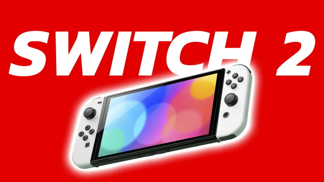
While the Japanese company hasn’t officially announced anything about the successor to the Nintendo Switch (hence the name, and for lack of a better idea, we’ll call it Switch 2, unless it’s Switch U after Wii U…), rumors are already out there.
Earlier this week, we reported on Nvidia’s T239 SOC (system-on-a-chip), which may use the Ampere architecture (GeForce RTX 3000). The processor, meanwhile, can rely on Arm. Two insiders, Kopite7kimi and Revegnus, are also sure that Nintendo will use Samsung’s 8-nanometer technology. The former claims that SEC8N will be used to manufacture the T239, while the latter suspects the more advanced solution, 7LPH. It seems similar to TSMC’s 4N node used by Nvidia (N5, a more advanced version of the 5-nanometer technology…).
More modern technology would also impact price, so it’s unfortunate to be optimistic, but you never know what Nvidia might be working on. Maybe Nintendo will get an even better architecture and/or chip design. (Ada Lovelace?) The successor to the Switch could have 1280 CUDA cores, claims KittyYYuko. Ampere has two versions: the HPC version has 64 cores per SM, while the consumer version has a 128/SM configuration, so there could be 10 SMs in the device. According to Kipite7kimi, the T239 is based on one GPC, while the Orin SOC is based on two (each with 8 SMs and 1024 cores, which would be 16/2048 total). Nvidia also had a GPC with 10 SMs in the GA106 GPU, but that could be something different, or they could turn off some SMs on the chip.
The processor is said to have 8 Cortex A78 Arm cores; of these, the C variant might be used. There is a maximum of 8 MB of L3 cache in these, but the version used on the Orin A78AE had 2 MB per quad-core cluster, so the total for the 12 cores was 6 MB. And in another video, we hear that the Switch successor uses 5-nanometer technology, capable of clock speeds up to 2.5GHz. The video’s creator found this from a LinkedIn profile: he worked at Siliconist Technologies from February 2020 to October 2022 and was a physical design engineer on Nvidia’s T239 project. The T239 could be the SoC for Switch 2. The 5nm, 2.653 GHz clock speed (higher than the clock speed of Tegra X1, the Switch’s SoC) has been profiled.
To put it more plainly, the Switch 2 will not get the latest graphics technologies (if the SoC were Ada-based, it would be capable of DLSS 3). Still, since it cannot use regular desktop hardware, it must compress the processor and the graphics chip into a single system board (see also handheld PCs). All the while, power consumption must be considered, so compromises have to be made somewhere. And all of it is not yet official.


![A God of War-Style Game With a Ballerina Fighting Slavic Gods Actually Exists, and Tsarevna: Age of Tales Already Looks Wild Enough to Stand Out [VIDEO]](https://thegeek.games/wp-content/uploads/2026/04/theGeek-Tsarevna-Age-of-Tales-302x180.jpg)


![A God of War-Style Game With a Ballerina Fighting Slavic Gods Actually Exists, and Tsarevna: Age of Tales Already Looks Wild Enough to Stand Out [VIDEO]](https://thegeek.games/wp-content/uploads/2026/04/theGeek-Tsarevna-Age-of-Tales-300x365.jpg)
Leave a Reply